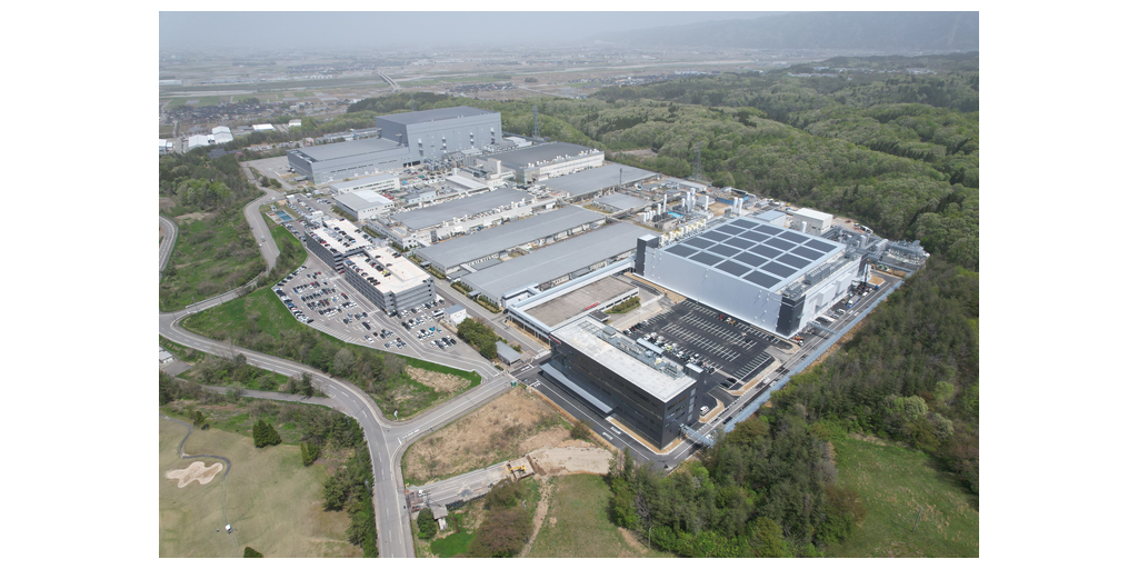
KAWASAKI, Japan–(BUSINESS WIRE)–Toshiba Electronic Devices & Storage Corporation (“Toshiba”) today held a ceremony to mark the completion of a new 300-millimeter wafer fabrication facility for power semiconductors and an office building at Kaga Toshiba Electronics Corporation in Ishikawa Prefecture, Japan, one of Toshiba’s key group companies. The completion of construction is a major milestone for Phase 1 of Toshiba’s multi-year investment program. Toshiba will now proceed with equipment installation, toward starting mass production in the second half of fiscal year 2024. Once Phase 1 reaches full-scale operation, Toshiba’s production capacity for power semiconductors, mainly MOSFETs[1] and IGBTs[2], will be 2.5 times that of fiscal 2021, when the investment plan was made[3]. Decisions on the construction and start of operation of Phase 2 will reflect market trends.
The new manufacturing building follows and will make a major contribution to Toshiba’s Business Continuity Plan (BCP): it has a seismic isolation structure that absorbs earthquake shock and redundant power sources. Energy from renewable source and solar panels on the roof of the building (onsite PPA model) will allow the facility to meet 100% of its power requirement with renewable energy.
Product quality and production efficiency will be boosted by the use of artificial intelligence (AI). Toshiba expects to receive a grant from the Ministry of Economy, Trade and Industry of Japan to subsidize its investment in part of the manufacturing equipment.
Power semiconductors play a crucial role in electricity supply and control, and are essential devices for energy efficiency in all electrical equipment. With the continuing electrification of automobiles and the automation of industrial machinery, they are expected to see continued robust demand growth. Toshiba started power semiconductor production on a new 300-millimeter wafer line in the second half of fiscal 2022 at Kaga Toshiba Electronics’ existing facility. Going forward, the company will expand production with the new fab and further contribute to carbon neutrality.
[1] Metal-Oxide-Semiconductor Field-Effect Transistor
[2] Insulated Gate Bipolar Transistor
[3] The total of 200- and 300-millimeter wafer fabrication capacity (200-millimeter equivalent)
Overview of Kaga Toshiba Electronics Corporation
Location: 1-1, Iwauchi-machi, Nomi-shi, Ishikawa Prefecture, Japan
Established: December, 1984
President and Representative Director: Satoshi Aida
Employees: 1,150 (as of March 31, 2024)
Main Products: Discrete semiconductors (power semiconductors, small-signal devices and optoelectronic devices)
Web: https://www.toshiba-kaga.co.jp/ (Japanese only)
* Information in this document, including product prices and specifications, content of services and contact information, is current and believed to be accurate as of the date of the announcement, but is subject to change without prior notice.
* Company names, product names, and service names mentioned herein may be trademarks of their respective companies.
About Toshiba Electronic Devices & Storage Corporation
Toshiba Electronic Devices & Storage Corporation, a leading supplier of advanced semiconductor and storage solutions, draws on over half a century of experience and innovation to offer customers and business partners outstanding discrete semiconductors, system LSIs and HDD products.
Find out more at https://toshiba.semicon-storage.com/ap-en/top.html
Contacts
Media Inquiries:
Toshiba Corporation
Media Relations Office, Corporate Communications Div.
Phone +81-3-3457-2100
Mail [email protected]


